
Overview of PCB Footprint Expert
Table of Contents
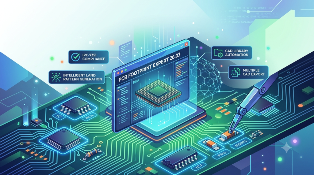
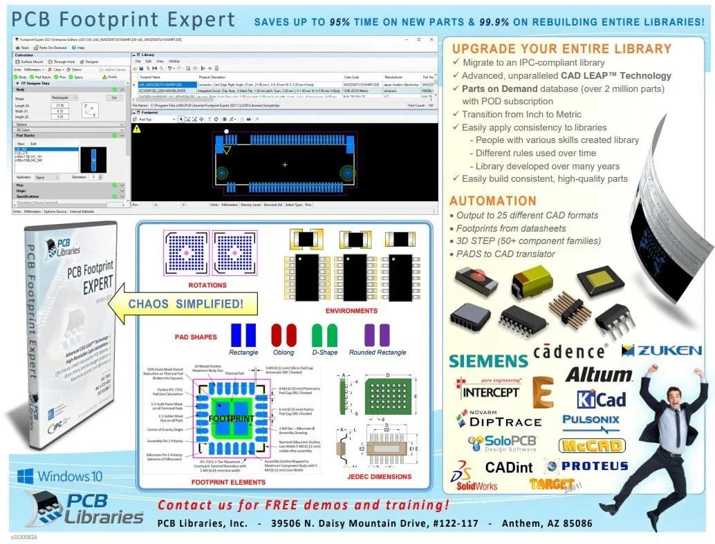
PCB Footprint Expert is the industry’s original IPC footprint automation solution, providing a rule-based approach to library development that ensures consistency across organizations and projects. Unlike manual footprint creation methods, which are prone to human error and inconsistent standards, this software empowers users to generate complete component libraries based on predefined or customizable rules.
The tool supports both surface mount and through-hole component families, offering extensive flexibility for designers working on everything from simple two-layer boards to complex high-density designs. With its advanced CAD LEAP™ (Libraries Enhanced with Automated Preferences) technology, Footprint Expert delivers libraries that are compliant with key industry standards, including IPC-7352, IPC-7351, and IPC J-STD-001. This ensures that all generated footprints meet quality benchmarks for solder joint reliability and manufacturability.
Key Differentiators:
-
Rule-Based Automation: Reduces manual effort and ensures consistency across libraries.
-
Multi-CAD Support: Outputs to over 25 different CAD formats, including Altium Designer, Allegro, KiCad, PADS, and Xpedition.
-
Industry Compliance: Automatically generates footprints compliant with IPC and IEC standards.
-
Flexible Customization: Offers over 1,800 customizable parameter combinations to meet specific design requirements.
Key Features
Multi-CAD Format Compatibility
Footprint Expert supports library creation in a wide range of PCB design tools, making it a versatile solution for design teams working across different environments. Supported formats include:
-
Allegro (Cadence)
-
Altium Designer / Altium Nexus
-
KiCad
-
PADS and Xpedition (Siemens)
-
OrCAD PCB
-
EAGLE
-
DipTrace
-
Proteus, Pulsonix, and TARGET 3001 as well as others.
5-Tier Density Variation Support
The software provides five distinct density levels to accommodate different product applications:
-
IPC A (Maximum): For low-density products, offering the widest process window for soldering.
-
IPC B (Median): For moderate-density products, balancing robustness and space efficiency.
-
IPC C (Minimum): For high-density portable and handheld devices, minimizing board space.
-
User-Defined Preferences: Customizable standards for organization-wide consistency.
-
Manufacturer-Recommended Footprints: Pre-defined patterns optimized for specific components.
3D STEP Model Generation
Footprint Expert automatically generates accurate 3D STEP models directly from component dimensions. This eliminates the need for manual 3D modeling, ensuring that design teams have precise representations of components for mechanical integration and visualization.
Pad Stack and Library Management
Users have full control over pad stack definitions, including:
-
Support for Rectangle, Oblong, D-Shape, and Rounded Rectangle pad shapes.
-
Thermal Tab configuration with options for paste mask reduction and corner radius apertures.
-
Pad stack naming conventions that intelligently avoid redundant identifiers.
The built-in library editor includes robust management functions:
-
Search, edit, and save capabilities for efficient part management.
-
Custom data fields (corporate part numbers, pricing, supplier information, etc.).
-
Duplicate part number detection to maintain library integrity.
What’s New in Version 26.03
Version 26.03, released in March 2026, includes several fixes and enhancements to improve the accuracy, usability, and performance of the software.
3D STEP Enhancements
-
Updated Polarized Chip Capacitor: Improved 3D modeling for polarized chip capacitors, ensuring more accurate representation in mechanical designs.
-
KiCad Terminal Outline Fix: Resolved an issue where terminal outlines were not registering correctly on pads when exporting to KiCad, improving compatibility.
FP Designer Improvements
-
Paste Mask Layer Fix: When adding a Paste Mask Layer to a through-hole pad stack for Pin-in-Paste applications, the software previously added the layer twice. This has been corrected in version 26.03.
-
BGA Pin Numbering Fix: Corrected an issue where automatic alphanumeric pin numbering for BGA components would start repeating after ‘BY’ (e.g., ‘BA’ after ‘BY’).
-
Silkscreen Outline Fix: Ensured that disabling the “Allow Expanded Outline” option in Drafting > Silkscreen is properly saved to the FPX file format.
Library Editor Fixes
-
Row Addition Fix: Corrected an issue where changing the number of rows in the Library Editor from 2 to 1 would still add 2 rows.
-
Duplicate Part Number Detection: Fixed a utility function that was displaying one fewer found duplicate than existed.
-
SON/PSON Description Cleanup: Removed redundant “Flat” terminology from SON and PSON component descriptions in both the user interface and FPX files.
Options and Calculators
-
Pad Stack Naming: Removed redundant mask pad shape identifiers (e.g., ‘C’, ‘R’) from pad stack names when they matched the top pad shape.
-
Thermal Tab Enhancements:
-
Added Thermal Tab Minimum Pattern to Pad Edge for better control over thermal pad design.
-
Enabled corner radius thermal pad paste mask apertures.
-
-
DPAK Improvements:
-
The ‘Pattern’ setting is now the default for DPAK thermal tab paste mask shapes.
-
The ‘Simple’ paste mask setting now correctly follows the Paste Mask Reduction percentage defined in Options.
-
-
SOIC/SOP Orientation Fix: Corrected zero-orientation communication for SOIC/SOP component families.
-
Calculator Reconciliation: Added reconciliation for two-pin parts with dissimilar terminal sizes and tolerances, ensuring consistent calculations regardless of pin location order.
System Requirements
PCB Footprint Expert is designed to run on Windows-based systems. While the official documentation primarily lists Microsoft Windows 8.1 64-bit Professional or Enterprise, and Windows 7 32 or 64-bit Pro, Enterprise, or Ultimate Editions, the latest versions are compatible with modern Windows operating systems.
Recommended Hardware Specifications
| Component | Recommended Specification |
|---|---|
| Operating System | Windows 10/11 64-bit (Professional or Enterprise) |
| Processor | Intel Core i7 or Xeon 2.66 GHz+ quad core (or equivalent AMD) |
| Memory (RAM) | 8 GB or higher |
| Disk Drive | 7200 RPM SATAIII or SSD; DVD drive (for installation media) |
| Graphic Adapter | OpenGL compatible, 256MB RAM minimum; 32-bit color at 1280×1084 or greater |
| Ethernet Card | Required for node-locked license management |
| Network | 100/1000 mbps for license server communication |
| Microsoft .NET Framework | Version 4.5 or later (required for installation) |
Installation Guide
This guide outlines the steps to install PCB Footprint Expert 26.03 on a Windows system. Always refer to the official documentation for the most current instructions.
Pre-Installation Checklist
-
Verify System Requirements: Ensure your system meets the minimum hardware and software specifications listed above.
-
Check .NET Framework: Confirm that Microsoft .NET Framework 4.5 or later is installed. If not, download and install it from Microsoft’s official website.
-
Disable Antivirus Temporarily (Optional): Some antivirus software may interfere with the installation. Temporarily disabling it can prevent installation errors. Re-enable it after installation.
-
Administrator Rights: You must have administrative privileges on the computer to install the software.
Step-by-Step Installation
-
Download the Installer:
-
Visit the PCB Libraries downloads page at
pcblibraries.com/downloads. -
Login or register for a free account.
-
Locate the Footprint Expert 26.03 installer and download the
Install_FootprintExpert26.03_Pro.exefile.
-
-
Run the Installer:
-
Double-click the downloaded
.exefile to launch the installation wizard. -
If prompted by User Account Control (UAC), click “Yes” to allow the installation.
-
-
Follow Installation Prompts:
-
Click “Next” on the welcome screen.
-
Read and accept the End-User License Agreement (EULA).
-
Select the installation directory (default is typically
C:\Program Files\PCB Libraries\Footprint Expert). -
Click “Next” to proceed.
-
-
Install:
-
The installer will copy files and configure the software. This may take a few minutes.
-
-
Complete Installation:
-
Once the installation finishes, click “Finish” to close the wizard.
-
License Activation
After installation, you need to activate your license. PCB Libraries offers several licensing options:
-
Evaluation License: For a fully functional trial, complete the evaluation request on the downloads page.
-
Leased License: For subscription-based access.
-
Perpetual License: A one-time purchase license that does not expire.
Activation Steps:
-
Launch the Footprint Expert application.
-
You will be prompted to activate your license.
-
Choose the appropriate activation method:
-
Enter License Key: Input the license key provided with your purchase.
-
Online Activation: The software can typically activate online if your computer has internet access.
-
Offline Activation: If the computer is offline, follow the instructions provided by PCB Libraries to generate an offline activation file.
-
-
Once the license is successfully activated, the software will be ready for use.
How to Use the Software
This section provides a practical workflow for creating a footprint using PCB Footprint Expert.
User Interface Overview
The Footprint Expert interface is designed with a clear and logical layout:
-
Component Family Menu: Choose the component type (e.g., Surface Mount, Through-hole).
-
Specification Input: Enter component dimensions, tolerances, and other parameters.
-
Graphic Preview: Real-time 2D and 3D visualization of the footprint.
-
Rules & Options: Configure pad settings, silkscreen preferences, and IPC density levels.
Basic Workflow
-
Launch and Set Preferences:
-
Open the software.
-
Before creating a footprint, configure your default preferences (units, pad shapes, rotations, origins) via the Options menu to match your organizational standards.
-
-
Select Component Family:
-
Choose the appropriate component family from the main menu (e.g., “Surface Mount”).
-
Select the specific sub-family (e.g., “Chip Capacitor”, “QFP”, “BGA”).
-
-
Enter Component Specifications:
-
Enter the component’s physical dimensions as provided in the manufacturer’s datasheet.
-
You can input data using nominal values with tolerances or minimum/maximum dimensions.
-
The software will automatically calculate the appropriate pad sizes and spacings based on the selected rules.
-
-
Choose IPC Density Level:
-
Select the desired density level:
-
A (Maximum): For low-density designs.
-
B (Nominal): For moderate-density designs.
-
C (Minimum): For high-density designs.
-
-
-
Review and Customize:
-
Examine the real-time preview to confirm the footprint looks correct.
-
Adjust advanced settings if necessary, such as:
-
Pad Shapes: Choose between Rectangle, Oblong, D-Shape, or Rounded Rectangle.
-
Pin 1 Orientation: Set per IEC 61188-7 or custom preferences.
-
Paste Mask and Solder Mask: Define swell and reduction values.
-
Thermal Tab Settings: Configure paste mask patterns and minimum pad edges.
-
-
-
Generate the Footprint:
-
Click the “Create Part” or “Generate” button to finalize the footprint.
-
The software will generate the pad stack, silkscreen outlines, assembly details, and courtyard.
-
-
Export to CAD:
-
Select the target CAD format (e.g., Allegro, Altium Designer, KiCad).
-
The software will output the footprint in the correct file format, ready to be imported into your PCB design tool.
-
Batch Processing: For generating multiple parts or entire libraries, use the batch processing feature to create an entire library at once, ensuring uniformity across all components.
-
Best Use Cases
1. Large-Scale Library Development
For companies building or migrating a component library from scratch, Footprint Expert automates the generation of thousands of footprints with consistent rules, ensuring that every footprint meets the same quality and compliance standards.
2. Compliance-Driven Design
When designing for industries with stringent regulatory requirements (e.g., aerospace, automotive, medical devices), the software’s built-in compliance with IPC-7352 and IPC J-STD-001 ensures that PCB libraries are audit-ready and support reliable solder joint formation.
3. Multi-CAD Design Environments
Design teams that use different CAD tools within the same organization can use Footprint Expert to maintain a single source of truth for libraries and output to multiple formats, ensuring consistency across different toolsets.
4. High-Density and Complex Component Design
For advanced components like BGA, QFN, and DPAK packages with thermal pads, the software provides the specific controls needed to generate accurate footprints that account for thermal management, paste mask reduction, and optimal pad geometries.
5. Training and Onboarding
The rule-based nature of the software ensures that even less experienced designers can generate professional-grade footprints by simply following the datasheet input process, standardizing the output regardless of individual skill levels.
Advantages and Limitations
Advantages
| Advantage | Description |
|---|---|
| Consistency | Eliminates variations caused by manual creation; ensures every footprint follows the same rules across all users and projects. |
| Accuracy | Generates footprints strictly based on datasheet specifications and IPC calculations, reducing the risk of manufacturing errors. |
| Productivity | Automates a time-consuming and error-prone task, significantly reducing design cycle times. |
| Compliance | Built-in IPC-7352 and J-STD-001 compliance ensures design reliability and manufacturability. |
| Flexibility | Over 180 customizable settings allow adaptation to virtually any company’s design requirements. |
| Multi-CAD Support | Outputs to 25+ formats, making it ideal for teams using diverse tools. |
| 3D Model Generation | Automatic STEP model creation eliminates separate 3D modeling steps. |
Limitations
| Limitation | Description |
|---|---|
| Learning Curve | While user-friendly, the extensive customization options can be overwhelming for beginners without proper training. |
| Cost | Full licenses may be a significant investment for small teams or individuals, though a free Calculator version is available. |
| Windows-Only | The software is designed exclusively for Windows-based systems, limiting use for Mac or Linux-based designers. |
| Dependency on Datasheets | Accuracy relies on the designer correctly entering component dimensions from datasheets. |
| Library Management | While the software generates footprints, integrating and managing them within an existing CAD library still requires organizational effort. |
Alternatives to PCB Footprint Expert
While Footprint Expert is a market leader, several alternatives exist for PCB footprint and library creation. A direct comparison is provided below.
| Tool / Method | Primary Use | Key Features | Compatibility | Typical Cost |
|---|---|---|---|---|
| Ultra Librarian | Web-based library tool | Symbols, footprints, and 3D models; output to 30+ formats; based on component data | Extensive CAD support | Subscription (varies) |
| SnapEDA | Web-based library service | Searchable library; symbols and footprints with IPC-7351 compliance; free and premium tiers | Various CAD formats | Freemium / Subscription |
| Manual CAD Creation (Altium, Allegro, KiCad) | Built-in CAD tools | Full control over footprint design; no automation or industry-standard checks | Single CAD platform only | Included in CAD license |
| LP Wizard | Legacy IPC tool | Similar automation to Footprint Expert (PCB Libraries acquired LP Wizard) | Limited formats after acquisition; now integrated into Footprint Expert | Discontinued; integrated into Footprint Expert |
| Free Footprint Calculator (PCB Libraries) | Basic tool | Simple IPC calculations and free 3D models; no CAD export | N/A | Free |
Why Footprint Expert Stands Out
Footprint Expert provides the most comprehensive combination of rule-based automation, multi-CAD support, and IPC compliance. Its batch processing capability and ability to generate entire libraries with consistent rules make it the superior choice for professional design teams, especially when compared to manual methods or limited web-based services.
Frequently Asked Questions
1. What is PCB Footprint Expert?
PCB Footprint Expert is a professional software tool that automates the creation of PCB footprints and libraries. It uses rule-based automation to generate IPC-7352 and IPC J-STD-001 compliant land patterns and 3D STEP models for over 25 CAD formats.
2. What’s new in PCB Footprint Expert version 26.03?
Version 26.03 includes several bug fixes and enhancements. Key updates include corrected paste mask layer generation for Pin-in-Paste, improved BGA alphanumeric pin numbering, fixes for KiCad and SON/PSON export, enhanced thermal tab and paste mask controls for SMD components, and improved calculator reconciliation for two-pin parts.
3. Is there a free version of PCB Footprint Expert?
A free evaluation version is available for a limited trial period. The free Footprint Calculator is also available for simple IPC calculations without CAD export. The full Pro version, with all CAD outputs, requires a paid license (starting at $149/year or perpetual licenses available).
4. What CAD formats does PCB Footprint Expert support?
PCB Footprint Expert supports over 25 CAD formats, including Allegro, Altium Designer, KiCad, PADS, Xpedition, OrCAD PCB, EAGLE, DipTrace, Proteus, Pulsonix, and TARGET 3001.
5. How do I install PCB Footprint Expert 26.03?
-
Download the installer from the PCB Libraries website.
-
Ensure Microsoft .NET Framework 4.5 or later is installed.
-
Run
Install_FootprintExpert26.03_Pro.exeand follow the installation wizard prompts. -
Activate your license by entering your license key or using online/offline activation methods.
6. What is the difference between the Footprint Expert and the Free Footprint Calculator?
The Free Footprint Calculator is a basic tool that allows users to calculate pad sizes based on IPC rules and view 3D models, but it does not export to CAD formats. The Footprint Expert (full version) includes all calculation features, plus CAD output generation for 25+ formats, batch processing, advanced customization, and library management tools.
7. Does PCB Footprint Expert generate 3D models?
Yes, Footprint Expert automatically generates accurate 3D STEP models directly from the component dimensions you input. These models are fully compatible with mechanical CAD software and are essential for 3D PCB visualization and mechanical integration analysis.
8. How does PCB Footprint Expert ensure PCB footprint compliance?
The software is built around the latest guidelines of IPC-7352, IPC-7351, and IPC J-STD-001. It also follows the IEC 61188-7 standard for component orientation. By using these standards as the basis for its calculation engine, it ensures all generated footprints meet industry requirements for manufacturing quality and reliability.
Final Thoughts
PCB Footprint Expert 26.03 is an essential tool for any hardware design team looking to improve efficiency, reduce errors, and ensure compliance in their PCB library development. By automating the generation of IPC-compliant footprints and 3D models across a wide range of CAD platforms, the software solves one of the most tedious and error-prone aspects of the PCB design process.
The latest version, 26.03, demonstrates a commitment to continuous improvement, with targeted bug fixes and enhancements that further refine its accuracy, usability, and multi-CAD compatibility. Whether you are building a library from scratch, migrating to a new CAD tool, or ensuring your designs meet rigorous industry standards, PCB Footprint Expert offers the automation, flexibility, and reliability needed to succeed.
For design teams committed to delivering high-quality, manufacturable PCBs, PCB Footprint Expert 26.03 represents a strategic investment in design quality and engineering productivity.
Our Paid Service
“We do not sell or provide any software. We only offer professional support services. If any software on your system is not working properly, or you are facing installation errors, crashes, or any other technical issue — just contact us. We will help you fix the problem quickly and remotely via AnyDesk. No software will be provided from our side — only expert troubleshooting and support.”